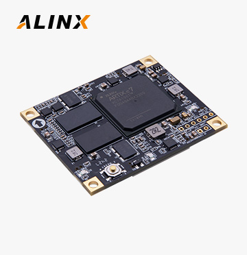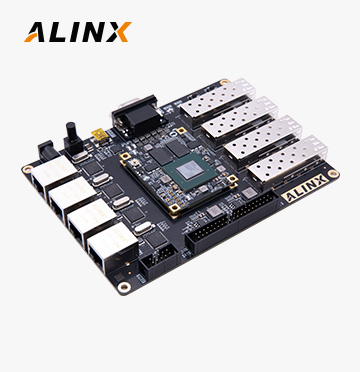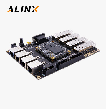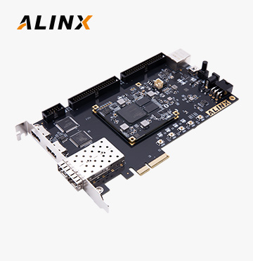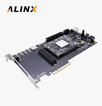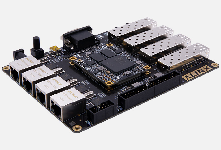


The AX7101 FPGA development board equipped with the AMD Artix 7 series device, delivers standout performance with DDR3 SDRAM, QSPI Flash, Gigabit Ethernet, SFP+, VGA out.
Unit price
$ 292In stock:
>9, ready to ship in 2 workdays

The AX7101/AX7201 FPGA development board equipped with the AMD/Xilinx Artix 7 series device, delivers standout performance with fast DDR3 SDRAM, QSPI Flash, Gigabit Ethernet, SFP+, VGA out.
Provide high-speed communication (SFP+) and video applications (VGA).
● communication
● Image and video processing
● Data analysis
● medical care
● Industrial control
● Network Information Security
Design-in Kit – The Fast Way to the Market, to get started with development straight out of the box.
The ALINX FPGA development board help shorten time-to-market for any AMD/Xilinx Artix 7 based application.

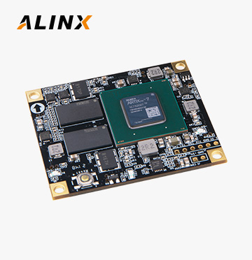
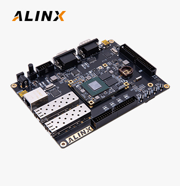
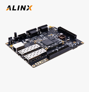
* The AX7101 development board consists of a AC7100B SoM and base board. If you want to purchase AC7100B SoM separately.
Please check the Relevant Products at the bottom of the page and click to learn more details.
| System-on-Module | 1 | Base Board | 1 |
|---|---|---|---|
| Mini USB Cable | 1 | USB Downloader Cable / set | 1 |
| 12V Power Adapter | 1 | Acrylic board | 1 |
| Heatsink | 1 |
1. For non-preferred models, a minimum order quantity (MOQ) may apply if the products are not in stock.
2. We offer custom configuration, a MOQ applies.
Please contact us for more details.
We offer complete documentations and a lot of demos and tutorials.
Please contact us should you have any need.
AX7101 User Manual
2023-04-25Links: AMD Pangomicro AUMO Autonomous Driving


Alinx Electronic Limited 沪ICP备13046728号
Please verify your email address by getting a code before downloading.