
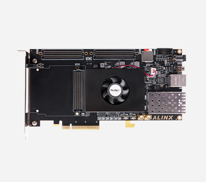
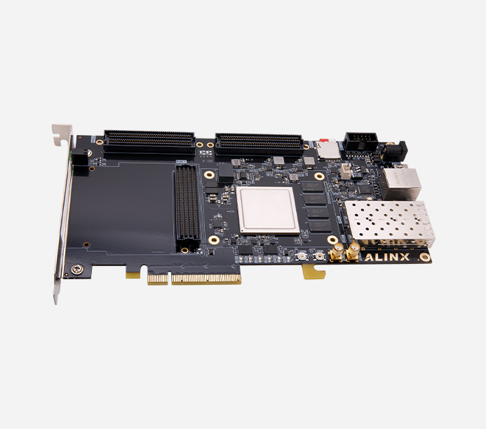
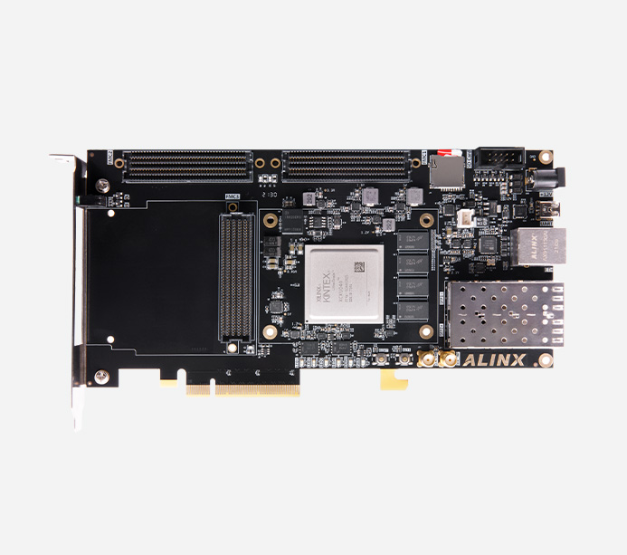


XCKU040
Model
AXKU041Ean
6971390279250Price
$ 924For high-speed data transmission and exchange, pre-verification and post-application of data processing is possible

Software version: all supporting materials of vivado 2017.4 development board are provided through Baidu online disk. After purchase, please contact customer service to obtain them
Basic experiment
01. LED water lamp experiment and simulation in vivado
02. Key Experiment in Vivado
03. Serial port Transmitting and Receiving experiment
04. Key Shake Removal Experiment
05. LM75 Temperature Test Routine
06. SD Card Read and Write Test Experiment
07.12C Interface EEPROM Experiment
08. DDR4 Read and Write Test Experiment
09. FPGA on-chip ROM Read and Write Test Experiment
10. FPGA on-chip RAM Read and Write Test Experiment
11. FPGA on-chip FIFO Read and Write Test Experiment
12. Gigabit Ethernet transmission experiment
13. GTH Fiber Optic Communication Testing Experiment
14. GTH Fiber Optic Communication Testing Experiment ⑵
15. Pcie Test routine
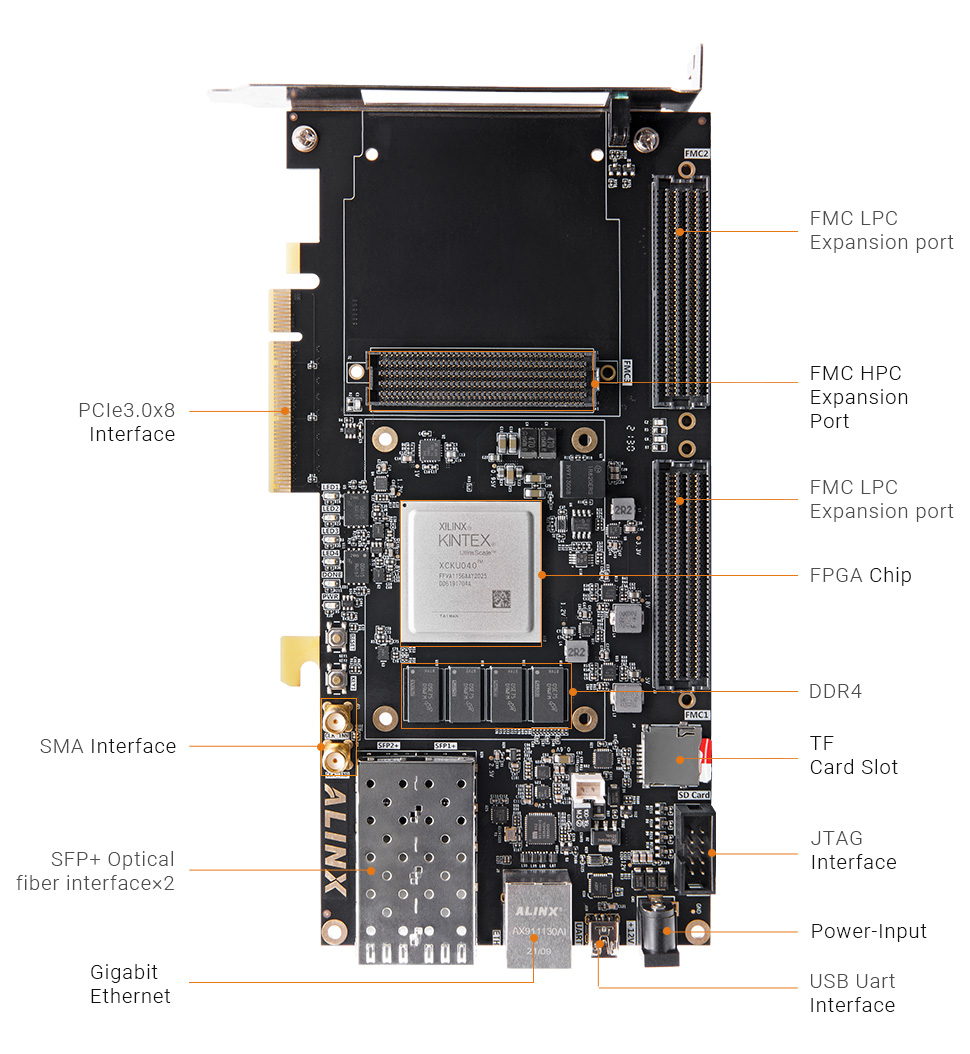
FPGA Chip
XCKU040-2FFVA1156I
Chip level
Industrial Grade
Logic Cells
530.250
Look Up Tables (LUTs)
242,400
CLB Flip-Flops
484,800
PCIe Gen3 x8
3
Block RAM (Mb)
21.1
DSP Slices
1920
Transceiver
20X 12.5Gb/s max
Speed class
-2
DDR4
4x 1GB DDR4
QSPI Flash
Two 256Mbit 64MB QSPI flash memory chips can be used to store FPGA chip configuration files and user data
Optical fiber interface
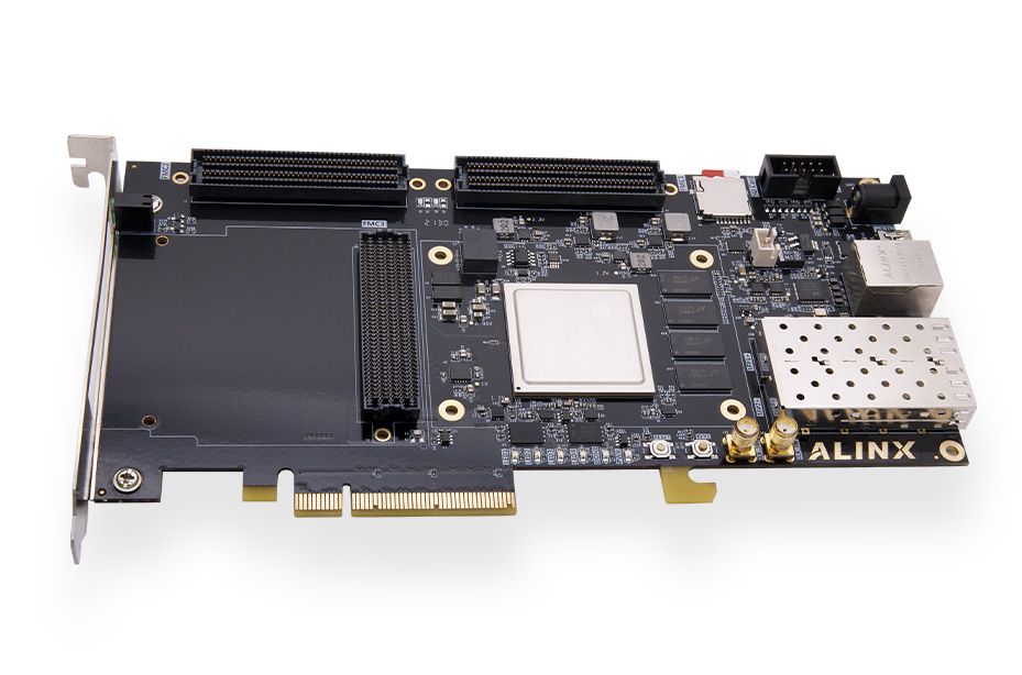
2-way SFP + optical fiber interface to realize 2-way high-speed optical fiber communication interface. The receiving and transmitting speed of each channel of optical fiber data communication is as high as 12.5Gb/s
FMC Extension interface
Three standard FMC expansion ports, including two LPC expansion ports and one HPC expansion port. External Xilinx or alinx FMC daughter boards (HDMI input and output module, binocular camera module, high-speed AD module, etc.)
SD Card Slot
1-way Micro SD card holder for data read, write and storage of SD card by GA
USB Uart
1 Uart to USB interface for communication with computer and user debugging
Ethernet interface
One 10/100m/1000m Ethernet RJ45 interface is used for Ethernet data exchange with computers or other network devices
SMA interface
2-way SMA External Interface for External High Speed Input and Output Signals
JTAG
10-pin 2.54mm standard JTAG port for downloading and debugging of field programmers
Crystal Oscillator
A 200Mhz differential crystal oscillator provides a stable clock source for the field bus system
A 125Mhz differential crystal oscillator to provide a reference clock for optical fiber
A 156.25Mhz differential crystal oscillator, which gives the transceiver a reference clock
Temperature Sensor
Sensor Chip LM75, Used to Detect the Ambient Temperature
EEPROM
One EEPROM for LC bus communication and storage of customer-defined information
LEDs
6 LEDs, 1 power indicator; One done configuration indicator, four user indicators, and a pair of panel indicators
KEYs
2 user keys, 1 reset key, 1 ordinary IO connected to FPGA
Voltage Input
+12V DC
Current Input
Max. Current 3A
FPGA Board
1
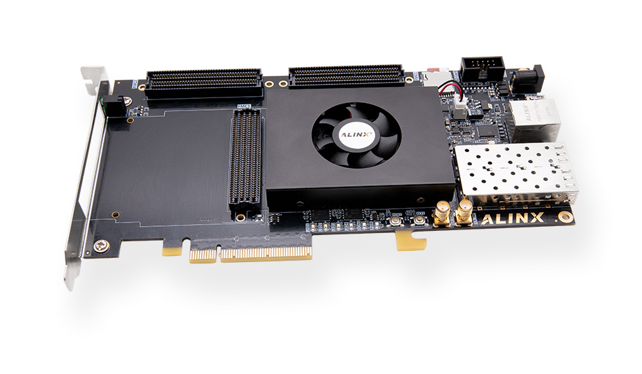
DC Fan (Fixed on the Board)
1
Mini USB Cable
1
USB Downloader Cable
1 Set
12V Power Adapter
1
Size Dimension
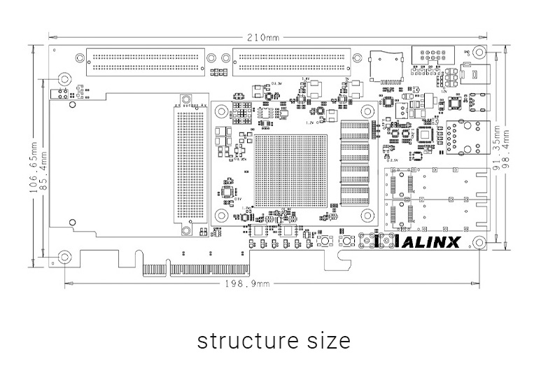
210mm x 106.65mm
Number of Layers
14-Layer Carrier Board PCB Reserve independent power layer and GND layer
High speed optical fiber communication, video processing, high-speed data transmission processing, etc
Support the requirements of high-speed data transmission and exchange, data storage, video transmission processing and industrial control, and the verification in the early stage of project development
Rich peripheral interfaces: 1 FMC HPC interface, 2 FMC LPC interfaces, 2 SFP+ optical fiber interfaces, 1 Gigabit Ethernet interface, 1 UART serial interface, 1 SD card interface, 1 road network interface, 2 SMA interfaces, 1 10-pin JTAG interface
Receiving and Transmitting Speed up to 12.5Gb/s
The warranty period of all products sold is 12 months, of which FPGA chips and LCD screens are wearing parts and are not covered by the warranty. All accessories and gifts are not covered under warranty.