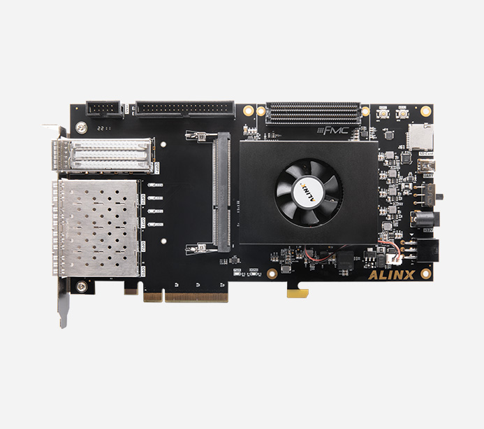


XC7K325
Model
AX7325BEan
6971390271742Price
$ 660
PCIe Acceleration Data, Optical Fiber Communication High-speed Data Transmission,Video Image Acquisition and Processing, Industrial Control

Supporting Verilog HDL Demos and Docuemnts . All Doucments Saved in Dropbox, after buy the board, email to get it.
00. Vivado 2017.4 Installation
01. LED water lamp experiment and Simulation in vivado
02. Key detection experiment in Vivado
03. PLL Experiment in Vivado
04. Serial port Transmitting and Receiving Experiment
05. Key debounce experiment
06. LM75 Temperature Test Experiment
07. SD Card Read and Write Experiment
08. HDMI Programming Output Experiment
09. DDR3 Read Write and Simulation Experiment
10. Recording and playback Experiment of AN831 Module
11. SD Card Music Player Experiment
12. Character Display Experiment
13. SD Card Read BMP Picture Display Experiment
14. OV5640 Camera Display Experiment
15. SOBEL Edge Detection Experiment
16. AD9238 Waveform Dispaly Experiment
17. AD7606 Waveform Display Experiment
18. ADDA Testing Experiment
19. 125M multi-channel AD test Experiment
20. AD9767 Waveform Display Experiment-Dual Channel Sine Wave Experiment
21. AD9767 Waveform Display Experiment-Dual Channel Triangle Wave Experiment
22. Gigabit Ethernet Transmission Experiment
23. AD9238 Chip Ethernet Communication
24. AD7606 Chip Ethernet Transmission Experiment
25. AD9280 Chip Ethernet Communication
26. Gigabit Ethernet Video Transmission Experiment
27. GTX Fiber Optic Communication IBERT Testing Experiment
28. GTX Fiber Optic Data Communication Experiment
29. Video Image GTP Fiber Optic Transmission Experiment
30. Video Image GTX Fiber Optic CommunicationTesting Experiment
31. PCIe Speed Test Experiment
32. PCIe HDMI Input Experiment
33. PCIe HDMI Output Experiment
34. PCIe xdma Interface Experiment
35. PCIe ADC Transfer Experiment
FPGA Board
AN831 Audio Package
Optical Module Package
AN9767 Collection Package
AN706 Collection Package
AN9238 Collection Package
Video Package
Luxury Package
FPGA Board
●
●
●
●
●
●
●
●
USB Downloader
●
●
●
●
●
●
●
●
FL9134
●
●
●
●
●
●
AN831
●
●
Optical Module
●
●
AN9767
●
●
AN706
●
●
AN9238
●
●
Binocular Camera
●
●
4.3-inch LCD
●
●
Supporting Modules in the Package, Click to Learn More

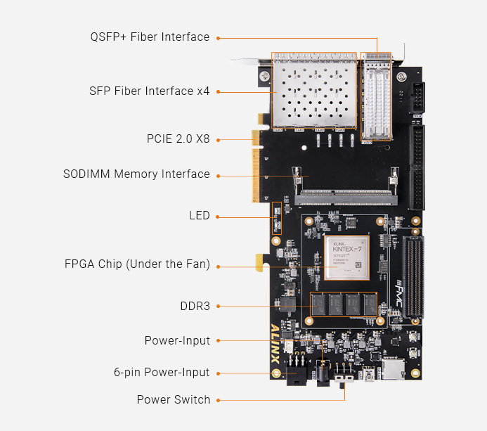
FPGA Chip
XC7K325T-2FFG900I
PCIe Gen2
X8
Logic Cells
326,080
Transceiver
16× 12.5Gb/s max
Look Up Tables ( LUTs )
50,950
CLB Flip-Flops
407,600
Block RAM
16,020Kb
DSP
840
Temperature class
Industrial Grade , -40℃-85℃
Speed Grades
-2
XADC
1× 12bit 1Mbps AD
DDR3
2GB DDR3, 64bit Bus, Data Rate 1600Mbps
QSPI Flash
128Mbit, Used as FPGA Configuration File and User Data Storage
Crystal Oscillator
Two 200Mhz differential clocks provide reference clocks for DDR controllers
Two differential clocks, 125Mhz and 156.25Mhz respectively, are high-speed transceivers GTX
Partial provision of differential clock source
Transceiver
16 GTP, each up to 12.5Gb/s, Used for SFP and PCIe Data Communication
PCIe x8
Support PCI Express 2.0 Standard, Standard PCIe x 8 High-Speed Data Transmission Interface. Each rate can be up to 8GBaud
SFP
4 SFP Interfaces, the Speed of Each Channel is up to 10Gb/s
QSFP+
QSFP+ Interface, the Speed of Each Channel is up to 40Gb/s
SODIMM Memory
SODIMM Memory Interface, for DDR3 memory, data width 64 bits
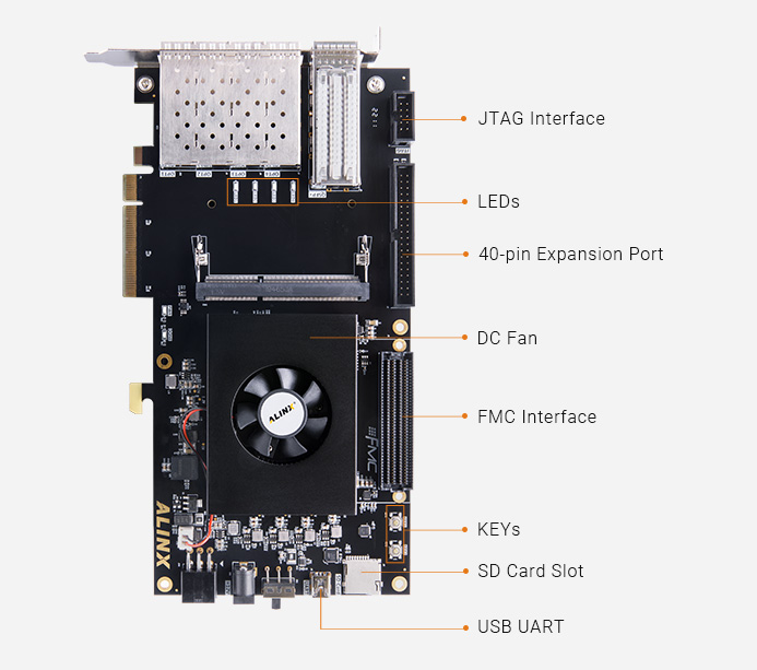
JTAG
Standard JTAG Port for Debug and Download of FPGA Program
Temperature Sensor
Temperature Sensor chip LM75, used to detect the temperature of the environment around the board
FMC Port
Standard FMC LPC Expansion Port Can be Connect with Various XILINX or ALINX FMC Modules (HDMI, Camera, Hight Speed AD Modules)
USB Uart
Used for Serial Communication with PC or External Devices
LED
1 Power Indicator; 1 DONE Configuration Indicator 4 FPGA Control Indicators
SD Card Slot
Micro SD Card Slot, Support the SD Mode and SPI Mode
40-Pin Expansion Ports
Reserved 40-Pin Expansion Ports (0.1 inch Pitch), Can be Connect with Various ALINX Modules (Binocular Camera Module, TFT LCD Screen, Camera, AD/DA and Other Modules)
KEYs
2 User Keys
Voltage Input
+12V DC
Current Input
Max. Current 3A
FPGA Board
1
DC Fan (Fixed on the Board)
1
Mini USB Cable
1
USB Downloader Cable
1 Set
12V Power Adapter
1
PCIe Fence
1
Size Dimension
221mm x 120mm
Number of Layers
FPGA Development Board 12-Lay PCB

Optical Fiber Communication, PCIe Acceleration Video Processing, Industrial Control High-Speed Data Transmission Processing

PCIe x8, 4X 10G SFP, 40G QSPF +, USB UART, SD Card Slot, FMC Standard Expansion Port, 40-pin Expansion ports
Meet the PCIe Acceleration Data, Optical Fiber Communication, High-speed Data Transmission, Video Image Acquisition and Processing and Industrial Control Requirements.
For the Pre-verification and Post-application of High-Speed Video Transmission and Exchange, High-Speed Optical fiber Communication and PCIe Data Processing
Verify PCIE Solution Speed up PCIE Product Development

Collect the Video Signal through the FL9134 HDMI Input Interface Upload it to the Computer Through the PCIE Interface, and Display the Video Image in Real Time

The Host Computer Grabs the Computer Desktop, and Transmits it to the FPGA through the PCIE Interface. The FPGA Outputs through the FL9134 HDMI Interface,The Monitor Displays in Real Time
Meet Various PCIe High-Speed Data Transmission Video Image Processing Needs

Industrial Control, Video Image Acquisition and High-Speed Transmission Processing

SFP 10G Transceiver Communication Eye Diagram

QSFP+ 40G Transceiver Communication Eye Diagram
Intelligent Identification, Medical Security Vehicle Digital, Industrial Control, Smart Grid

Dual Lens Camera Module On-Board Demo
The Binocular Camera Module AN5642 for Video Capture Displays it on the Display through the HDMI Interface of the External FL9134 Daughter Board to Realize Binocular Display Simultaneously.
Expand the storage space and data bandwidth of Board Support up to 8GB Micron, Data rate 800Mbps

Memory Module Needs to be Purchased Separately
AN9767 / AN706 Module On-Board Demo

*The Signal Source Output Signal is Connected to the AN9767 Module, and the Waveform Signal is Displayed through the Oscilloscope
*The Signal Source Output Signal is Connected to the AN706 Module, Run the System to Draw the Waveform Data, and is Displayed to the Monitor through the HDMI Interface of the FPGA Development Board
The warranty period of all products sold is 12 months, of which FPGA chips and LCD screens are wearing parts and are not covered by the warranty.
All accessories and gifts are not covered under warranty.