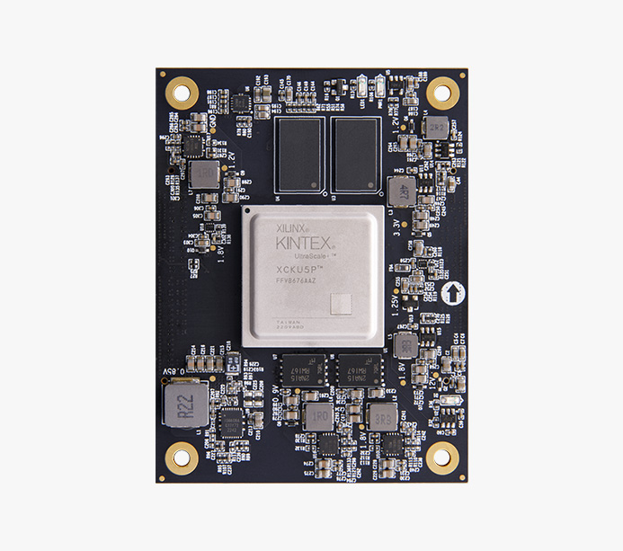
XCKU5P
Model
ACKU5Temperature class
-40℃~85℃Price
$ 660
Kinex UltraScale+device adopts a 16nm process, which significantly reduces power consumption by 60% compared to the 7-series FPGA. Especially the GTY 28Gb/s x16 transceiver and 100G Ethernet provide a cost-effective solution for applications that require high-end functionality. It is an ideal choice for applications such as wireless MIMO technology, Nx100G wired networking, and data center networking and storage acceleration, video image processing, semiconductors, industrial control, machine vision, the Internet of Things, and medical imaging.
475K
434K
217K
28Gb/s x16
Support
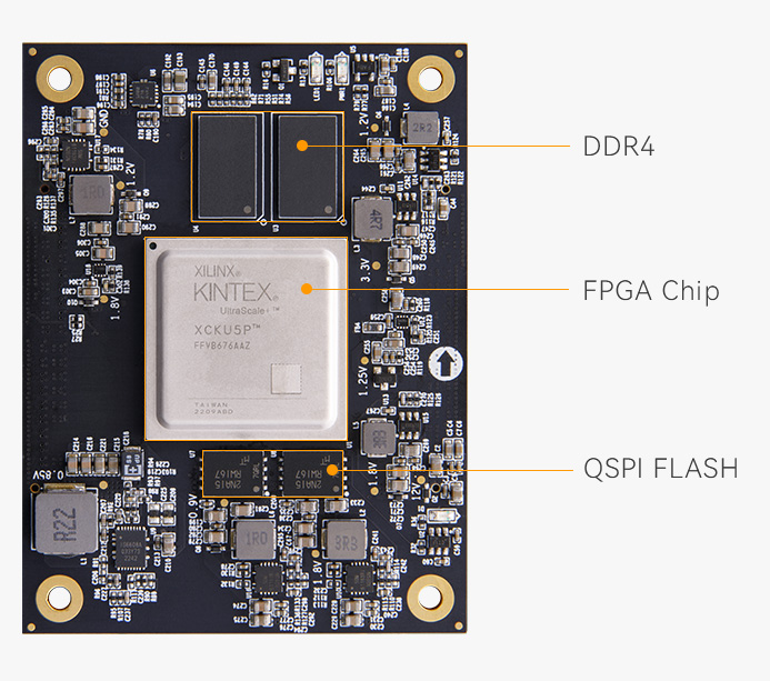
2GB DDR4 32bit,64MB QSPI FLASH


*Learn about the corresponding development board, Click to see details >>
Core Board Chip
ACKU3
ACKU5
FPGA Chip
XCKU3P-2FFVB676I
XCKU5P-2FFVB676I
Chip Level
Speed Grades -2,Industrial Grade, -40°C~85°C
Speed Grades -2,Industrial Grade, -40°C~85°C
DDR4
2GB DDR4, 32bit
2GB DDR4,32bit
QSPI FLASH
64MB
64MB
System Logic Cells
356K
475K
CLB Flip-Flops
325K
434K
CLB LUTs
163K
217K
Max. Distributed RAM
4.7Mb
6.1Mb
Total Block RAM
12.7Mb
16.9Mb
UltraRAM
13.5Mb
18.0Mb
Clock Mgmt Tiles
4
4
DSP Slices
1,368
1,824
GTY Transceivers
GTY 28Gb/s x16
GTY 28Gb/s x16
PCI Express
PCIe Gen3 x16
PCIe Gen3 x16
100G Ethernet
-
1
HD IOs
72
72
HP IOs
96
96
LVDS
45
45
DDR4
Two 1GB DDR4 storage chips with a data rate of up to 2666Mbps
QSPI Flash
Two 32MB QSPI FLASH chips, storing FPGA configuration Bin files and other user data files
Clock configuration
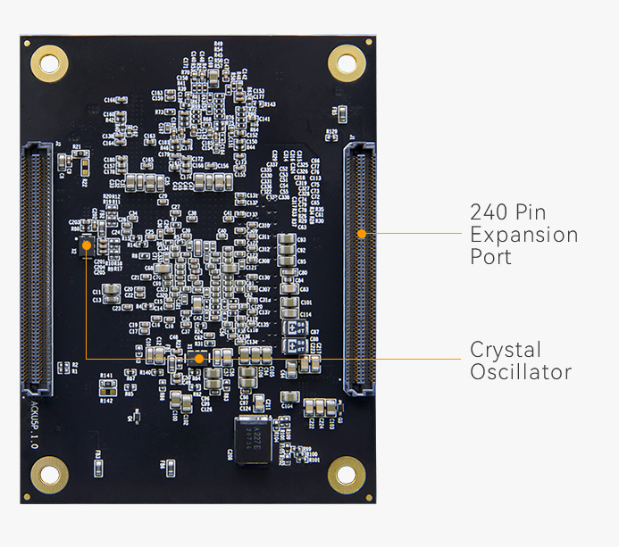
Two 200MHz differential crystal oscillators are provided on the board, which can provide reference clocks for DDR4 controllers and FPGA logic
240pin connector
Two 240Pin high-speed expansion ports have been used to expand 179 IOs using two 240Pin inter board connectors, and the level of the IO output can be modified
LED lights
1 is the power indicator light (PWR1), 1 is the configuration LED light (D1), and 1 is the user indicator light (LED1)
Voltage Input
+12V, powered by connecting the backplane
FPGA SoM Board
1
Size Dimension
3.15inch * 2.36inch * 0.378inch
Number of Layers
14-Layer Core Board PCB,Reserve independent power supply layer and GND layer

Structural dimension diagram


Provide Schematic, PCB, Size Dimension, Package and Reference Design, that to Accelerate the Development of products with Core Board


Network Communication

Data Center Networking and Storage Acceleration

Medical Imaging

Industrial Automation

Video Imaging

IOT

ATE

Machine Vision
The warranty period of all products sold is 12 months, of which FPGA chips and LCD screens are wearing parts and are not covered by the warranty. All accessories and gifts are not covered under warranty.